Research
Magic-Angle Twisted Bilayer Graphene
When two sheets of monolayer graphene are rotated relative to one another, a moiré pattern emerges (see image below). At a twist angle of 1.1°, the newly formed periodicity greatly modifies the electronic properties of the graphene sheets, giving rise to superconductivity, correlated insulators, and magnetic behavior. We worked on understanding these exotic phases of matter in twisted bilayer graphene by measuring its electronic excitation spectrum as a function of energy and electron density.

See Nature 582, 198-202 (2020), Nature 588, 610-615 (2020), Nature 600, 240-245 (2021), Nature 620, 525-532 (2023), and Physical Review B 92, 155409 (2015) for our work on twisted bilayer graphene.
Engineering Electric Potentials in Graphene
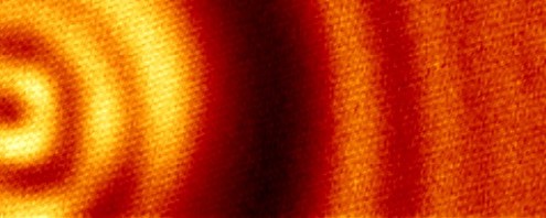
Electrons in monolayer graphene move as though they are relativistic massless particles that obey the two-dimensional (2D) Dirac equation. Thus, graphene provides an excellent simulator for the physics of high-energy electrons. By manipulating charged defects, we created various electrostatic potentials (such as the Coulomb potential and the harmonic-oscillator potential) in graphene and imaged the resulting electronic wavefunctions. Here is a density-of-states image of a standing wave of electrons confined in graphene:
See Nature Physics 12, 1032-1036 (2016) and Science 340, 734-737 (2013) for our work on controlling and imaging Dirac fermions in graphene.
Quantum Spin Hall States in 1T'-WTe2 and 1T'-WSe2
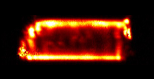
A topological insulator is a material that is insulating in its interior but conductive on its boundary. In two dimensions, this implies dissipationless current-carrying edges that are robust against disorder. We studied the Quantum spin Hall edge states of transition-metal dichalcogenides 1T'-WTe2 and 1T'-WSe2. Below is a conductance map of a 1T'-WSe2 domain showing enhanced density of states at its edges.
See Nature Physics 13, 683–687 (2017) and Nature Communications 9, 3401 (2018) for our work on 1T'-WTe2 and 1T'-WSe2.
Scanning Tunneling Microscopy
Scanning tunneling microscopy (STM) is a powerful tool for characterizing surfaces with atomic-scale resolution. By applying a voltage bias between a conducting tip and a surface, electrons are extracted from or injected into the surface via quantum tunneling. Measuring the tunneling current provides energy-resolved electronic-structure information about the material. Additionally, STM images can be Fourier transformed to obtain momentum-space data. Here is a time-lapse of the construction of our STM.
See Review of Scientific Instruments 91, 023703 (2020) for information about the STM that we built.